Content Menu
● The Fundamentals of Silicon Carbide
● Industrial Manufacturing Methods
>> 1. The Acheson Process
>> 2. Physical Vapor Transport (PVT)
>> 3. Chemical Vapor Deposition (CVD)
● Modern Innovations in Silicon Carbide Mass Production
>> AI-Driven Process Optimization
>> Large Furnace Technology
>> Recycling and Sustainability
● Applications of Mass-Produced Silicon Carbide
● Challenges in Industrial-Scale Production
● Future Trends
● Conclusion
● FAQ
>> 1. Why is silicon carbide preferred over silicon in power electronics?
>> 2. How long does it take to grow a single SiC crystal using PVT?
>> 3. What percentage of global SiC production uses the Acheson process?
>> 4. Can silicon carbide be recycled?
>> 5. What's the main barrier to wider SiC adoption in semiconductors?
Silicon carbide (SiC) has become a cornerstone material for industries requiring extreme durability, thermal stability, and electrical efficiency. Its mass production leverages advanced industrial processes refined over decades, combining high-temperature synthesis, precision engineering, and cutting-edge automation. This article explores the methodologies, challenges, and innovations driving silicon carbide mass production, providing insights into its critical role across sectors like energy, defense, and advanced manufacturing.
The Fundamentals of Silicon Carbide
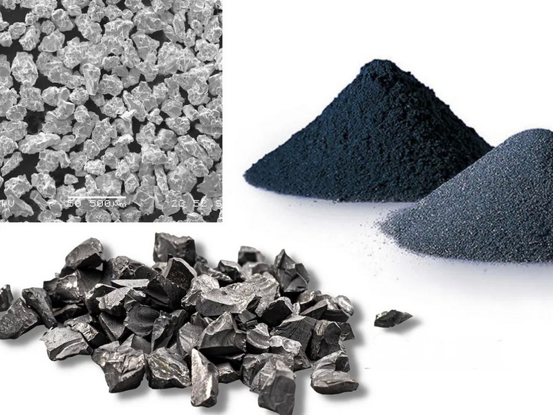
Silicon carbide is a synthetic compound of silicon and carbon, renowned for its exceptional hardness (9.5 Mohs), thermal conductivity (120–490 W/m·K), and chemical inertness. Unlike naturally occurring moissanite, industrial SiC is produced synthetically to meet stringent purity and structural requirements.
Industrial Manufacturing Methods
1. The Acheson Process
Developed in 1891 by Edward Acheson, this method remains the most widely used for bulk SiC synthesis.
Steps:
1. Raw Material Preparation: High-purity silica sand (SiO₂) and petroleum coke (C) are mixed in a 1:3 ratio.
2. Furnace Assembly: The mixture is loaded into a graphite-lined electric resistance furnace.
3. Reaction Phase: Temperatures exceeding 2,500°C trigger the reaction:
SiO2+3C→SiC+2CO
4. Cooling & Extraction: After 36–48 hours, the furnace cools, and crude SiC crystals are extracted from the graphite core.
5. Crushing & Grading: The material is pulverized and sorted into grit sizes for abrasives, refractories, or further processing.
Advantages:
- Cost-effective for large-scale output.
- Suitable for abrasive and metallurgical-grade SiC.
Limitations:
- Energy-intensive (up to 12 MWh per ton).
- Limited purity (95–98%) due to residual impurities like iron and aluminum.
2. Physical Vapor Transport (PVT)
PVT dominates the production of single-crystal SiC wafers for electronics.
Steps:
1. Sublimation: SiC powder is heated to ~2,400°C in a vacuum, vaporizing into Si, Si₂C, and SiC₂ gases.
2. Crystal Growth: Vapors condense on a cooler seed crystal, forming a single-crystal ingot.
3. Wafer Processing: The ingot is sliced into wafers using diamond wire saws and polished to nanoscale smoothness.
Advantages:
- Produces 4H-SiC and 6H-SiC crystals for power devices.
- Enables doping (e.g., nitrogen for n-type, aluminum for p-type).
Challenges:
- Slow growth rates (0.2–2 mm/hour).
- High defect density compared to silicon.
3. Chemical Vapor Deposition (CVD)
CVD deposits ultra-pure SiC layers onto substrates like graphite or silicon.
Steps:
1. Gas Introduction: Silane (SiH₄) and methane (CH₄) are fed into a vacuum chamber.
2. Thermal Decomposition: At 1,200–1,600°C, gases react to form SiC on the substrate:
SiH4+CH4→SiC+4H2
3. Layer Thickness Control: Process duration determines coating thickness (1–100 µm).
Applications:
- Protective coatings for turbine blades.
- Mirror substrates for space telescopes.

Modern Innovations in Silicon Carbide Mass Production
AI-Driven Process Optimization
- Temperature Control: Machine learning algorithms adjust furnace parameters in real-time, reducing energy use by 15%.
- Defect Detection: Computer vision systems identify crystal imperfections during PVT growth, improving yield by 30%.
Large Furnace Technology
- Scaling Acheson furnaces to 10-meter lengths increases batch output by 400%.
- Automated charging systems reduce labor costs and contamination risks.
Recycling and Sustainability
- CO emissions from Acheson reactors are captured and converted to formic acid.
- SiC sludge from wafer cutting is repurposed for refractory bricks.
Applications of Mass-Produced Silicon Carbide
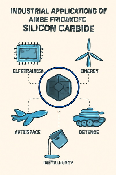
| Industry | Use Case | Benefit |
| Electronics | EV inverters | 10x higher switching efficiency |
| Energy | Solar panel inverters | 25% reduced energy loss |
| Aerospace | Turbine blade coatings | 1,500°C oxidation resistance |
| Defense | Armor plating | Stopping power vs. 20mm AP rounds |
| Metallurgy | Crucibles for molten metal | 3x longer lifespan vs. alumina |
Challenges in Industrial-Scale Production
1. Energy Costs: 60% of SiC production expenses stem from electricity.
2. Crystal Defects: Dislocations in PVT-grown wafers limit device yields.
3. Graphite Supply: 80% of high-purity graphite comes from China, creating supply chain risks.
Future Trends
- 8-Inch Wafer Adoption: Transitioning from 150mm to 200mm wafers could cut chip costs by 35%.
- Liquid Phase Epitaxy: Emerging techniques promise defect-free SiC layers at 1,800°C.
Conclusion
Silicon carbide mass production has evolved from artisanal batch processes to highly automated systems capable of delivering both megatons of abrasive grit and defect-free 200mm wafers. As renewable energy and electric vehicles drive demand, manufacturers are investing $4 billion annually to refine crystal growth techniques, adopt Industry 4.0 technologies, and secure raw material supplies. With its unmatched combination of thermal, electrical, and mechanical properties, SiC stands poised to revolutionize industries from quantum computing to hypersonic aviation.

FAQ
1. Why is silicon carbide preferred over silicon in power electronics?
SiC's wider bandgap (3.3 eV vs. 1.1 eV) enables operation at higher temperatures and voltages, reducing energy losses by up to 70% in EV inverters.
2. How long does it take to grow a single SiC crystal using PVT?
A 150mm-diameter 4H-SiC boule typically requires 7–10 days of continuous growth at 2,200°C.
3. What percentage of global SiC production uses the Acheson process?
Approximately 75% of abrasive-grade and 40% of metallurgical-grade SiC rely on Acheson furnaces.
4. Can silicon carbide be recycled?
Yes, up to 90% of SiC grinding wheels are recycled into refractory materials or road abrasives through crushing and magnetic separation.
5. What's the main barrier to wider SiC adoption in semiconductors?
Wafer costs remain 5–8x higher than silicon due to complex crystal growth and lower yields, though prices are falling 15% annually.


