Content Menu
● Introduction to Silicon Carbide
● Overview of Silicon Carbide Production Methods
● The Acheson Process
>> Principle and Steps
● The Lely (Sublimation) Process
>> Principle and Steps
● Chemical Vapor Deposition (CVD)
>> Principle and Steps
● Physical Vapor Transport (PVT)
>> Principle and Steps
● Reaction-Bonded Silicon Carbide (RBSC)
>> Principle and Steps
● Polymer-Derived Ceramics (PDCs)
>> Principle and Steps
● Modern Improvements and Automation
● Quality Control in Silicon Carbide Production
● Applications of Silicon Carbide
● Environmental Impact and Sustainability in Silicon Carbide Production
● Future Trends in Silicon Carbide Production
● Conclusion
● FAQ
>> 1. What is the most common method for producing silicon carbide?
>> 2. How is high-purity silicon carbide produced for electronic applications?
>> 3. What are the benefits of chemical vapor deposition (CVD) in silicon carbide production?
>> 4. How does reaction-bonded silicon carbide differ from other methods?
>> 5. What quality control measures are used in silicon carbide production?
Silicon carbide (SiC) is a critical material in modern industry, renowned for its exceptional hardness, thermal conductivity, chemical stability, and semiconducting properties. It is indispensable in sectors such as abrasives, refractories, electronics, automotive, aerospace, and energy. The demand for high-quality silicon carbide continues to rise, driving innovation in its production methods. This article provides a comprehensive overview of the main silicon carbide production methods, their principles, advantages, and modern technological advancements.
Introduction to Silicon Carbide
Silicon carbide is a compound of silicon and carbon, occurring naturally as the rare mineral moissanite but produced synthetically for industrial use. Its unique combination of mechanical, thermal, and electronic properties makes it suitable for a wide range of applications, from abrasives and cutting tools to high-power semiconductors and advanced ceramics.
Overview of Silicon Carbide Production Methods
Several methods are used to produce silicon carbide, each tailored to specific purity, crystal size, and application requirements. The primary silicon carbide production methods include:
- The Acheson process (electric resistance furnace)
- The Lely process (sublimation growth)
- Chemical vapor deposition (CVD)
- Physical vapor transport (PVT)
- Reaction-bonded silicon carbide (RBSC)
- Polymer-derived ceramics (PDCs)
Each method offers unique benefits and is chosen based on the desired end-use of the silicon carbide product.
The Acheson Process
Principle and Steps
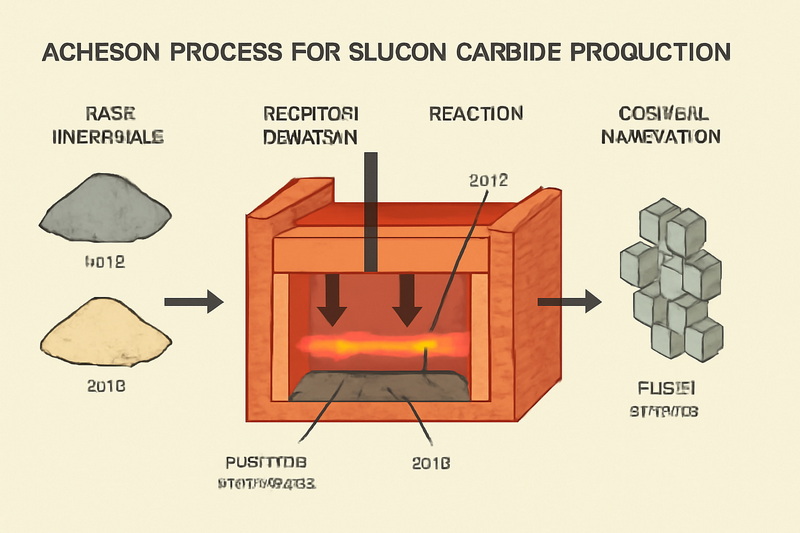
The Acheson process, developed in 1891, is the most widely used industrial method for producing silicon carbide. It involves the high-temperature reaction of silica (SiO₂) and carbon (usually from petroleum coke or coal) in an electric resistance furnace.
Process Steps:
1. Raw Material Preparation: Silica sand and carbon are mixed, sometimes with additives like sawdust (to increase porosity) and salt (to lower reaction temperature).
2. Furnace Loading: The mixture is loaded into a large, electrically heated graphite furnace.
3. Heating: The furnace is heated to temperatures between 2,000°C and 2,500°C. The reaction is:
SiO2+3C→SiC+2CO
4. Reaction and Crystal Growth: Silicon carbide crystals form around the graphite core, while carbon monoxide gas is released.
5. Cooling: The furnace is allowed to cool, and the solid mass (boule) is extracted.
6. Crushing and Grading: The boule is crushed and sorted by particle size for various applications.
7. Purification: For high-purity requirements, additional chemical or thermal purification steps are employed.
Advantages:
- Cost-effective and scalable
- Produces large quantities of SiC suitable for abrasives, refractories, and metallurgical uses
Limitations:
- High energy consumption
- Impurities may require further purification for electronic-grade SiC

The Lely (Sublimation) Process
Principle and Steps
The Lely process, or sublimation method, is used to grow high-purity single crystals of silicon carbide, essential for electronic and semiconductor applications.
Process Steps:
1. SiC Powder Loading: High-purity silicon carbide powder is placed in a graphite crucible.
2. Heating: The crucible is heated to around 2,500°C in an inert atmosphere (argon).
3. Sublimation: SiC powder sublimates (turns directly from solid to gas).
4. Crystal Growth: The vapor condenses on a cooler graphite seed rod, forming large single crystals.
Advantages:
- Produces high-purity, large single crystals
- Essential for semiconductor wafer production
Limitations:
- High cost and energy-intensive
- Slower growth rates compared to bulk production methods
Chemical Vapor Deposition (CVD)
Principle and Steps
Chemical vapor deposition is a technique for producing ultra-high-purity silicon carbide films and coatings, widely used in electronics and optics.
Process Steps:
1. Substrate Preparation: Cleaned substrates (often graphite or quartz) are placed in a CVD reactor.
2. Gas Introduction: Gaseous precursors (e.g., silane, methane, hydrogen) are introduced.
3. Reaction: At high temperatures, gases react and deposit SiC onto the substrate surface.
4. Film Growth: The thickness and composition are precisely controlled by adjusting gas flow and temperature.
5. Cooling and Removal: The SiC-coated substrate is cooled and removed for further processing.
Advantages:
- Produces extremely pure and uniform SiC films
- Allows for precise control over doping and thickness
Limitations:
- Expensive equipment and operational costs
- Typically suited for thin films, not bulk material
Physical Vapor Transport (PVT)
Principle and Steps
Physical vapor transport is a modern evolution of the Lely process, commonly used for growing large, high-quality SiC single crystals for semiconductor wafers.
Process Steps:
1. SiC Source Material: High-purity SiC powder is placed in a graphite crucible.
2. Seed Crystal Placement: A SiC seed crystal is positioned at the top of the crucible.
3. Heating: The system is heated to high temperatures (2,000–2,600°C) under controlled atmosphere.
4. Sublimation and Deposition: SiC powder sublimates and deposits onto the seed crystal, growing a large, defect-free boule.
Advantages:
- Enables production of large-diameter SiC wafers (up to 6 inches or more)
- High crystalline quality and purity
Limitations:
- Requires precise temperature control and advanced equipment
- High capital and operational costs
Reaction-Bonded Silicon Carbide (RBSC)
Principle and Steps
Reaction-bonded silicon carbide is produced by infiltrating a porous carbon or SiC preform with molten silicon, which reacts to form additional SiC.
Process Steps:
1. Preform Preparation: A mixture of SiC and carbon is shaped into the desired form.
2. Infiltration: The preform is infiltrated with molten silicon at temperatures above 1,400°C.
3. Reaction: Silicon reacts with carbon to form additional SiC, bonding the structure.
4. Cooling and Finishing: The product is cooled and machined as needed.
Advantages:
- Produces complex shapes and high-strength components
- Lower processing temperatures compared to some other methods
Limitations:
- Residual free silicon may affect properties
- Not suitable for high-purity electronic applications
Polymer-Derived Ceramics (PDCs)
Principle and Steps
Polymer-derived ceramics involve shaping preceramic polymers and then pyrolyzing them to form silicon carbide.
Process Steps:
1. Polymer Shaping: Preceramic polymers (e.g., polycarbosilanes) are shaped by casting, extrusion, or molding.
2. Pyrolysis: The shaped polymer is heated in an inert atmosphere (1,000–1,100°C), converting it to SiC ceramic.
3. Post-processing: Further densification or machining as required.
Advantages:
- Enables production of complex shapes and fibers
- Lower processing temperatures
- Useful for advanced composites and coatings
Limitations:
- Typically results in amorphous or nanocrystalline SiC
- May require additional processing for high-density applications
Modern Improvements and Automation
Advancements in temperature control, automation, and process monitoring have dramatically improved the efficiency, quality, and scalability of silicon carbide production. Key innovations include:
- Precise temperature management: Multi-segment gradient control and real-time feedback ensure uniform crystal growth.
- Automation and robotics: AI-assisted control and robotic handling increase yield and reduce defects.
- Continuous feed and improved crucible design: Enable larger crystals and higher throughput.
- Sustainable sourcing: Use of recycled silicon and byproducts reduces environmental impact.
Quality Control in Silicon Carbide Production
Stringent quality control is essential to ensure that silicon carbide meets the demanding requirements of modern applications. Key quality assurance steps include:
- Crystal quality inspection: X-ray diffraction, microscopic analysis, and dislocation density measurement
- Purity testing: Chemical composition analysis, impurity content, and atomic spectroscopy
- Performance verification: Electrical, thermal, and mechanical property testing
- International certification: Compliance with SEMI, JEDEC, and ISO 9001 standards
Applications of Silicon Carbide
Silicon carbide's unique properties make it indispensable in:
- Abrasives: Grinding wheels, sandpaper, cutting tools
- Refractories: Kiln furniture, crucibles, furnace linings
- Electronics: Power devices, Schottky diodes, MOSFETs, wafers for semiconductors
- Automotive: Electric vehicle power modules, brake discs, clutches
- Aerospace: Turbine blades, heat exchangers, rocket nozzles
- Energy: Nuclear fuel cladding, high-temperature filters, solar inverters
Environmental Impact and Sustainability in Silicon Carbide Production
As the demand for silicon carbide grows, so does the importance of sustainable production practices. Modern manufacturers are increasingly focusing on reducing the environmental footprint of silicon carbide production. This includes optimizing energy consumption, recycling raw materials, and minimizing waste emissions. For example, some facilities have implemented closed-loop systems to capture and reuse carbon monoxide gas generated during the Acheson process, reducing greenhouse gas emissions.
Efforts are also being made to develop water-efficient cooling systems and to recycle spent furnace linings and other byproducts. The adoption of renewable energy sources for powering electric furnaces is another emerging trend, further reducing the carbon footprint of silicon carbide production methods. These sustainability initiatives not only help protect the environment but also enhance the long-term viability and competitiveness of manufacturers in the global market.
Future Trends in Silicon Carbide Production
Looking ahead, silicon carbide production is poised to benefit from advances in nanotechnology and materials science. Researchers are exploring novel synthesis methods such as microwave-assisted heating and plasma-enhanced chemical vapor deposition to improve efficiency and material properties. Additionally, the integration of artificial intelligence in process control promises to enhance yield, reduce defects, and lower production costs.
Emerging research is also focused on developing additive manufacturing techniques for silicon carbide, enabling the creation of highly complex geometries and customized components. As demand for high-performance power electronics and energy-efficient devices continues to rise, the industry is expected to see further innovation in both silicon carbide production methods and applications.
Conclusion
Silicon carbide production methods have evolved to meet the diverse and demanding needs of modern industry. From the time-tested Acheson process to advanced techniques like CVD, PVT, and polymer-derived ceramics, each method offers unique advantages in terms of purity, crystal size, and application suitability. Ongoing innovations in automation, temperature control, and quality assurance continue to drive improvements in efficiency, cost, and product performance. As the demand for high-performance materials grows, silicon carbide's role in enabling technological progress is set to expand even further. The industry's focus on sustainability and emerging technologies ensures that silicon carbide production methods will remain at the forefront of advanced materials manufacturing for years to come.

FAQ
1. What is the most common method for producing silicon carbide?
The most common method is the Acheson process, which involves reacting silica sand and carbon in an electric resistance furnace at high temperatures to produce silicon carbide crystals. This method is widely used for bulk production of SiC for abrasives, refractories, and metallurgical applications.
2. How is high-purity silicon carbide produced for electronic applications?
High-purity silicon carbide is typically produced using the Lely (sublimation) process or physical vapor transport (PVT). These methods sublimate SiC powder and deposit it onto a seed crystal, resulting in large, defect-free single crystals suitable for semiconductor wafers.
3. What are the benefits of chemical vapor deposition (CVD) in silicon carbide production?
CVD enables the production of extremely pure and uniform silicon carbide films with precise control over thickness and doping. This is essential for advanced electronic, optical, and coating applications where material purity and uniformity are critical.
4. How does reaction-bonded silicon carbide differ from other methods?
Reaction-bonded silicon carbide (RBSC) is produced by infiltrating a porous preform with molten silicon, which reacts with carbon to form additional SiC. This method is ideal for creating complex shapes and high-strength components but may leave residual free silicon.
5. What quality control measures are used in silicon carbide production?
Quality control includes crystal quality inspection (X-ray diffraction, microscopy), purity testing (chemical and atomic analysis), performance verification (electrical and mechanical tests), and compliance with international standards such as SEMI, JEDEC, and ISO 9001.


