Content Menu
● Understanding Silicon Carbide Production
>> What is Silicon Carbide?
>> Key Production Methods
● Major Efficiency Challenges in Silicon Carbide Production Plants
● Strategies to Improve Efficiency in a Silicon Carbide Production Plant
>> 1. Optimize Raw Material Preparation
>> 2. Enhance Furnace and Reaction Control
>> 3. Implement Process Automation and AI
>> 4. Upgrade Crystal Growth Techniques
>> 5. Improve Shaping and Sintering Processes
>> 6. Advanced Packaging and Thermal Management
>> 7. Process Optimization with Machine Learning
>> 8. Quality Control and Yield Improvement
>> 9. Waste Reduction and Recycling
>> 10. Workforce Training and Continuous Improvement
● Innovations in Silicon Carbide Production Equipment
● Environmental Considerations and Sustainability
● Collaborative Research and Development
● Digital Twin Technology in Production Optimization
● Future Trends in Silicon Carbide Production
● Benefits of Improving Efficiency in Silicon Carbide Production
● Conclusion
● FAQ: Silicon Carbide Production Plant Efficiency
>> 1. What are the main steps in silicon carbide production?
>> 2. How can automation improve silicon carbide production efficiency?
>> 3. Why is wafer size important in SiC production?
>> 4. What role does AI play in process optimization?
>> 5. How can silicon carbide plants reduce energy consumption?
Silicon carbide (SiC) is a critical material for modern industry, powering advancements in sectors ranging from electronics and automotive to metallurgy, military, and energy. As demand for SiC grows, so does the pressure on silicon carbide production plants to improve efficiency, reduce costs, and deliver higher-quality products at scale. This comprehensive guide explores proven strategies, technological innovations, and process optimizations that can dramatically enhance the efficiency of a silicon carbide production plant.
Understanding Silicon Carbide Production
What is Silicon Carbide?
Silicon carbide is a compound of silicon and carbon, renowned for its exceptional hardness, thermal stability, chemical resistance, and superior electrical properties. These characteristics make it indispensable for:
- Abrasives and cutting tools
- High-temperature ceramics
- Power electronics and semiconductors
- Structural materials in aerospace and defense
- Petrochemical and mining equipment
Key Production Methods
The most common methods for producing silicon carbide include:
- Acheson Process: High-temperature reaction of silica and carbon in an electric resistance furnace, forming SiC crystals.
- Lely Method: Sublimation and recrystallization for high-purity SiC single crystals.
- Chemical Vapor Deposition (CVD): Gas-phase reaction for semiconductor-grade SiC.
- Physical Vapor Transport (PVT): Used for growing large, high-quality SiC crystals for wafers.
Major Efficiency Challenges in Silicon Carbide Production Plants
Before implementing improvements, it's crucial to recognize the main bottlenecks:
- High Energy Consumption: Traditional SiC synthesis requires temperatures above 2000°C, leading to significant energy costs.
- Slow Crystal Growth: SiC crystals grow slowly, especially in high-purity applications, limiting throughput.
- Material Loss and Defects: Impurities, non-uniform growth, and breakage reduce usable yield.
- Complex Shaping and Sintering: SiC's hardness complicates machining, shaping, and finishing, increasing processing time.
- Automation Gaps: Manual intervention in process control and material handling can introduce errors and slow down production.
Strategies to Improve Efficiency in a Silicon Carbide Production Plant
1. Optimize Raw Material Preparation
- Use High-Purity Inputs: Select and process silicon and carbon sources to minimize impurities, which can reduce defects and improve product quality.
- Automated Mixing and Sieving: Implement automated systems for precise mixing and particle size control, ensuring consistency in feedstock.
2. Enhance Furnace and Reaction Control
- Advanced Temperature Management: Employ multi-zone, real-time temperature control systems to maintain optimal reaction conditions, reducing energy waste and improving crystal quality.
- Energy Recovery Systems: Integrate heat exchangers to recover and reuse waste heat from furnaces, lowering overall energy consumption.
3. Implement Process Automation and AI
- Automated Process Monitoring: Use sensors and AI-driven analytics for real-time monitoring and adjustment of key parameters such as temperature, pressure, and gas flow.
- Robotic Handling: Deploy robots for tasks like crystal pulling, material transport, and wafer slicing to reduce manual errors and increase throughput.
- Predictive Maintenance: AI can forecast equipment failures, allowing for proactive maintenance and less downtime.
4. Upgrade Crystal Growth Techniques
- Epitaxial Growth: Favor epitaxial growth on substrates over direct ingot cutting, as it allows for faster, more uniform mass production and reduces material waste.
- Larger Wafer Sizes: Transition from 150mm to 200mm wafers to increase the number of chips per wafer by up to 80%, dramatically improving output and cost efficiency.
5. Improve Shaping and Sintering Processes
- Precision Shaping: Use advanced shaping techniques such as dry pressing, isostatic pressing, or injection molding for complex geometries.
- High-Efficiency Sintering: Adopt rapid sintering technologies and optimize sintering profiles to reduce cycle times while maintaining product density and strength.
6. Advanced Packaging and Thermal Management
- Innovative Packaging: Utilize advanced packaging methods (e.g., double-sided cooling, internal bus bars, copper clip attachments) to reduce parasitic inductance, improve thermal management, and enhance device reliability.
- Direct Cooling Solutions: Integrate direct cooling designs (like pin-fin heat sinks) in power modules to sustain high performance at elevated temperatures.
7. Process Optimization with Machine Learning
- Neural Network Modeling: Apply machine learning models (e.g., BP neural networks) to optimize process parameters such as insulation time, temperature, and material ratios, maximizing mechanical properties and minimizing defects.
- Optimization Algorithms: Use advanced algorithms (e.g., Butterfly Optimization Algorithm, Sparrow Search) to find ideal process combinations, improving strength and yield.
8. Quality Control and Yield Improvement
- Automated Inspection: Deploy automated optical and X-ray inspection systems for real-time defect detection and classification.
- Statistical Process Control (SPC): Implement SPC to monitor process stability and quickly address deviations, reducing scrap rates and improving overall yield.
9. Waste Reduction and Recycling
- Material Recycling: Recycle off-spec SiC and process byproducts back into the production cycle, reducing raw material costs and environmental impact.
- Reusable Substrates: Adopt substrate reuse technologies, allowing high-quality SiC wafers to be used multiple times, further lowering costs and improving sustainability.
10. Workforce Training and Continuous Improvement
- Skill Development: Regularly train staff on new equipment, process controls, and safety protocols.
- Lean Manufacturing: Apply lean principles to identify and eliminate waste in every stage of production, fostering a culture of continuous improvement.

Innovations in Silicon Carbide Production Equipment
The continuous advancement in production equipment plays a pivotal role in enhancing the efficiency of silicon carbide production plants. Modern equipment designs focus on improving energy efficiency, precision, and automation capabilities. For instance, the development of induction heating furnaces offers faster heating rates and more uniform temperature distribution compared to traditional resistance furnaces, significantly reducing energy consumption and improving product consistency.
Moreover, modular furnace designs allow for easier maintenance and scalability, enabling plants to adapt quickly to changing production demands without extensive downtime.
Environmental Considerations and Sustainability
Sustainability is becoming increasingly important in silicon carbide production. Plants are adopting greener technologies to minimize environmental impact. This includes using renewable energy sources, such as solar or wind power, to offset the high energy demands of SiC synthesis.
Additionally, advanced filtration and gas scrubbing systems are implemented to reduce emissions of harmful gases during the production process. Water recycling systems are also integrated to minimize water usage and waste.
By prioritizing sustainability, silicon carbide production plants not only comply with environmental regulations but also enhance their corporate social responsibility and market appeal.
Collaborative Research and Development
Collaboration between industry, academia, and research institutions accelerates innovation in silicon carbide production. Joint R&D projects focus on developing new materials, improving crystal growth techniques, and optimizing process parameters.
These partnerships facilitate knowledge exchange and provide access to cutting-edge technologies, helping plants stay competitive and responsive to market needs.
Digital Twin Technology in Production Optimization
Digital twin technology is emerging as a powerful tool for optimizing silicon carbide production. By creating a virtual replica of the production plant, operators can simulate different scenarios, predict outcomes, and identify potential issues before they occur.
This proactive approach enables better decision-making, reduces downtime, and enhances overall plant efficiency.
Future Trends in Silicon Carbide Production
Looking ahead, the silicon carbide industry is poised for significant growth driven by demand in electric vehicles, renewable energy, and high-frequency electronics. Future trends include:
- Integration of more AI and machine learning for autonomous process control.
- Development of even larger wafer sizes beyond 200mm.
- Advances in defect-free crystal growth techniques.
- Increased focus on circular economy principles, including material reuse and recycling.
Plants that embrace these trends will be well-positioned to lead the market and meet evolving customer requirements.
Benefits of Improving Efficiency in Silicon Carbide Production
- Lower Energy Costs: Advanced controls and energy recovery can reduce energy consumption by up to 70% in some process steps.
- Higher Throughput: Automation, larger wafers, and faster growth techniques enable more product output per unit time.
- Improved Product Quality: Tighter process control and advanced inspection reduce defects and ensure consistent high-quality SiC.
- Reduced Production Costs: Efficient resource use, recycling, and automation lower overall manufacturing costs.
- Greater Market Competitiveness: Efficient plants can respond faster to market demand and offer better pricing, securing a stronger position in the global SiC market.
Conclusion
Efficiency is the cornerstone of a successful silicon carbide production plant. By embracing advanced process controls, automation, machine learning, and innovative manufacturing techniques, SiC producers can dramatically improve yield, product quality, and profitability. As technology evolves, the integration of AI, larger wafer sizes, and sustainable practices will further transform the industry, enabling silicon carbide to meet the ever-growing demands of high-tech and industrial markets. Plants that prioritize innovation, sustainability, and continuous improvement will not only thrive but also set new benchmarks for excellence in the silicon carbide sector.

FAQ: Silicon Carbide Production Plant Efficiency
1. What are the main steps in silicon carbide production?
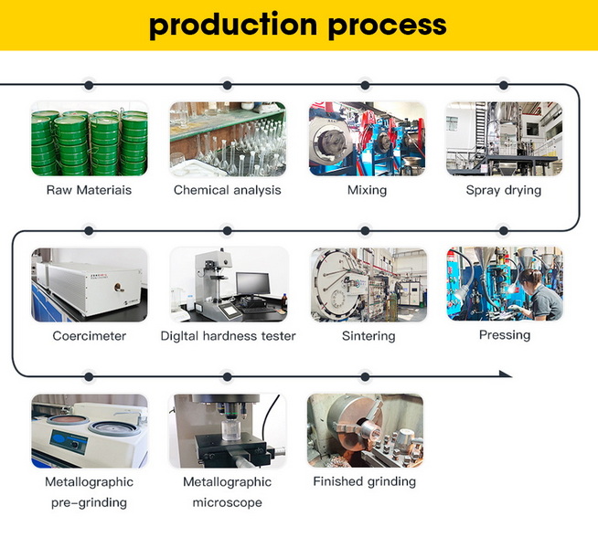
The main steps include raw material preparation, mixing, high-temperature reaction (e.g., Acheson process), cooling and separation, shaping (pressing or molding), sintering, and final finishing. For high-purity applications, crystal growth methods like the Lely method, CVD, or PVT are used, followed by wafer cutting and surface treatment.
2. How can automation improve silicon carbide production efficiency?
Automation streamlines material handling, process monitoring, and quality inspection. Automated systems reduce human error, enable real-time adjustments, and allow for continuous operation, increasing throughput and consistency while lowering labor costs.
3. Why is wafer size important in SiC production?
Larger wafer sizes (e.g., 200mm vs. 150mm) yield more chips per wafer, improve production efficiency, and reduce per-unit costs. The transition to larger wafers is a key trend in the industry, supporting higher demand and better economies of scale.
4. What role does AI play in process optimization?
AI and machine learning models can predict optimal process parameters, monitor equipment health, and detect anomalies. This leads to more stable processes, fewer defects, and higher yields, especially when dealing with complex, nonlinear production variables.
5. How can silicon carbide plants reduce energy consumption?
Plants can reduce energy use by integrating advanced temperature control systems, recovering waste heat, optimizing reaction profiles, and adopting energy-efficient equipment. Modern process improvements have demonstrated energy savings of up to 70% in some areas.


