Content Menu
● Types of Silicon Carbide Bonding
>> Reaction Bonding
>> Hydroxide Catalysis Bonding
>> Active Soldering
● Production Process Flow
>> Preform Fabrication
>> Silicon Supply Body Creation
>> Infiltration & Reaction
>> Post-Processing
● Industrial Applications
● Technical Challenges
>> 1. Thermal Management
>> 2. Porosity Control
>> 3. CTE Mismatch
>> 4. Surface Preparation
>> 5. Scale-Up and Consistency
● Advances in Silicon Carbide Bonding Technology
>> Microwave-Assisted Sintering
>> Laser Bonding
>> Additive Manufacturing Integration
>> Hybrid Bonding
● Environmental Impact and Sustainability
>> Recycling and Waste Reduction
>> Energy Efficiency
>> Life Cycle Considerations
● Quality Control and Testing
>> Non-Destructive Evaluation
>> Mechanical Testing
>> Thermal and Chemical Testing
● Future Trends and Research Directions
>> Nanostructured Silicon Carbide
>> Graphene-Reinforced Composites
>> Self-Healing Bond Interfaces
>> AI-Driven Process Optimization
>> Expanded Application Fields
● Conclusion
● FAQ
>> 1. How does silicon carbide bonding enhance component durability?
>> 2. What factors determine bonding method selection?
>> 3. Can bonded SiC withstand nuclear radiation environments?
>> 4. What safety precautions are essential during production?
>> 5. How do modern methods reduce production costs?
Silicon carbide (SiC) bonding is a critical process in manufacturing high-performance ceramic components used across industries like aerospace, defense, energy, and electronics. This technique creates durable molecular connections between silicon carbide particles or substrates, enabling exceptional thermal stability, mechanical strength, and chemical resistance. Three primary methods dominate industrial applications: reaction bonding, hydroxide catalysis bonding, and active soldering. Each approach addresses specific performance requirements in end products ranging from armor plating to semiconductor substrates.

Types of Silicon Carbide Bonding
Reaction Bonding
Reaction bonding is the most widely used method for producing dense silicon carbide components. This technique forms new silicon carbide through high-temperature reactions between silicon and carbon. A preform containing silicon carbide and carbon particles is infiltrated with molten silicon at temperatures typically between 1,410°C and 1,550°C under vacuum or inert gas. The liquid silicon reacts with carbon to create additional SiC, filling voids and strengthening the structure.
Key advantages include:
- Cost-effective production of complex shapes
- Minimal dimensional changes during processing
- High final density (up to 98% theoretical)
- Ability to produce large and intricate parts
Hydroxide Catalysis Bonding
Used for precision optical and semiconductor components, this room-temperature technique bonds oxidized SiC surfaces using alkaline solutions. A silica layer formed on SiC substrates reacts with hydroxide ions to generate siloxane bonds. The process preserves surface flatness within λ/10 (λ=633 nm), making it ideal for telescope mirrors and laser systems.
Key benefits:
- Extremely high bonding precision
- No need for high-temperature processing
- Maintains surface integrity and flatness
- Suitable for sensitive optical assemblies
Active Soldering
Metallurgical bonds between SiC and metals like stainless steel or copper are achieved using solder alloys containing reactive elements (e.g., titanium or zirconium). The solder chemically reacts with SiC surfaces at 220–450°C, enabling hermetic seals in cooling systems and power electronics.
Advantages:
- Enables joining of SiC with metals
- Lower processing temperatures compared to reaction bonding
- Useful for hybrid assemblies and electrical connections
Production Process Flow
Preform Fabrication
1. Raw Material Preparation:
Blend 1–10 μm SiC powder with 10–40 μm carbon black (0–30 vol%) and phenolic resin. The quality of the starting powders and their purity directly affect the final properties of the bonded SiC.
2. Granulation:
Dry or wet milling creates uniform particle mixtures, ensuring consistent distribution of carbon and silicon carbide throughout the preform.
3. Molding:
Compress granules at 5–400 MPa pressure to form near-net shapes. The molding process can be adapted for complex geometries, including honeycomb structures and intricate channels for heat exchangers.
Silicon Supply Body Creation
- Combine 70–99 wt% silicon powder (70–2,000 μm) with thermoset resins to form the silicon source.
- Thermoplastic additives (1–10 wt%) improve contact with uneven preform surfaces, ensuring complete infiltration during the reaction step.
Infiltration & Reaction
- Stack preforms and silicon bodies in sintering furnaces.
- Heat above silicon's melting point (1,410°C) under vacuum or inert atmosphere.
- Capillary action draws molten silicon into preforms, reacting with carbon to form new SiC. The infiltration process must be carefully controlled to avoid the formation of unreacted silicon pools and to achieve uniform density.
Post-Processing
Machining:
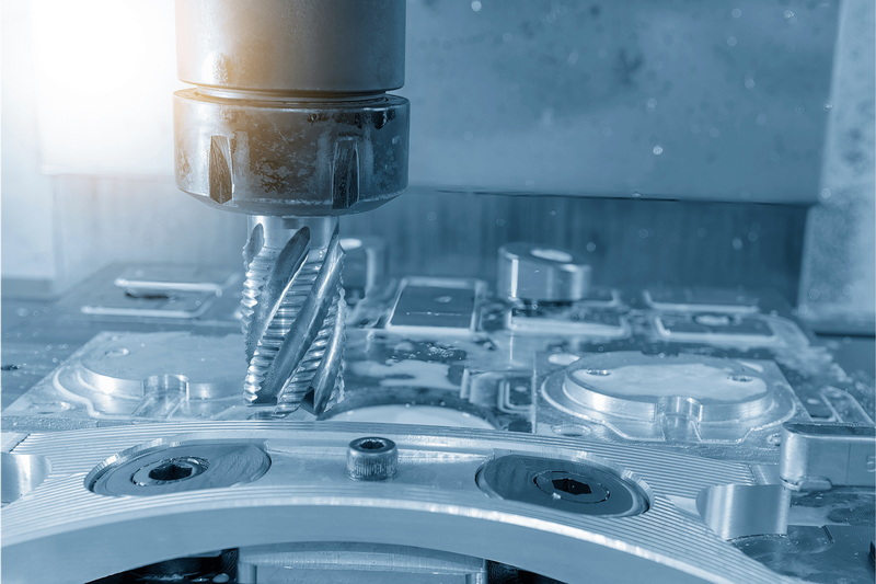
After bonding, components may require precision grinding or laser machining to achieve final tolerances and surface finishes.
Surface Treatments:
Additional coatings or polishing may be applied for enhanced corrosion resistance or optical performance.

Industrial Applications
| Sector | Use Case | Bonding Method |
| Defense | Armor plates | Reaction bonding |
| Electronics | Wafer chucks | Hydroxide catalysis |
| Energy | Heat exchanger tubes | Active soldering |
| Optics | Telescope mirror segments | Hydroxide catalysis |
| Automotive | EV power module substrates | Reaction bonding |
| Aerospace | Rocket nozzle throats | Reaction bonding |
| Chemical | Pump seals, valve seats | Reaction bonding |
| Mining | Drill bits, wear plates | Reaction bonding |
| Semiconductor | Substrate carriers | Hydroxide catalysis |
Technical Challenges
1. Thermal Management
Rapid exothermic reactions during silicon infiltration require precise temperature control to prevent warping and internal stresses. Advanced pyrometers with ±2°C accuracy monitor reaction zones in real-time. Uniform heating and controlled cooling rates are essential to avoid thermal gradients that can cause cracking or distortion.
2. Porosity Control
Unreacted silicon pools (5–15% by volume) must be evenly distributed to avoid mechanical weak points. X-ray tomography systems map pore distribution at 5 μm resolution, enabling manufacturers to optimize process parameters for minimal porosity and maximum mechanical strength.
3. CTE Mismatch
Differences in thermal expansion between SiC and metal components demand graded transition layers. Functionally graded materials (FGMs) with 10–100 μm layer thicknesses solve this issue, allowing for reliable joining of dissimilar materials in high-stress environments.
4. Surface Preparation
Hydroxide catalysis bonding requires oxide layers <100 nm thick with RMS roughness <1 nm. Atomic layer deposition (ALD) achieves 0.3 nm surface uniformity, which is crucial for achieving strong, defect-free bonds in optical and semiconductor applications.
5. Scale-Up and Consistency
Scaling up the silicon carbide bonding process for mass production introduces challenges in maintaining consistency across batches. Automated mixing, molding, and infiltration systems, along with real-time process monitoring, are becoming standard to ensure uniform quality.
Advances in Silicon Carbide Bonding Technology
Microwave-Assisted Sintering
Microwave-assisted sintering reduces processing times by 40% compared to conventional methods, operating at 2.45 GHz with 3–5 kW power output. This technology enables rapid, uniform heating, which minimizes grain growth and enhances mechanical properties.
Laser Bonding
Laser bonding techniques achieve localized heating rates of 10⁴°C/s, creating 50 μm wide bond lines with 450 MPa shear strength. This method is especially useful for microelectronic assemblies and joining small, delicate components.
Additive Manufacturing Integration
Additive manufacturing integration allows 3D-printed preforms with 200–500 μm wall thicknesses, reducing material waste by 60%. This approach enables the design and production of complex, lightweight structures that would be impossible with traditional manufacturing methods.
Hybrid Bonding
Hybrid bonding combines reaction bonding with active soldering to create multi-material components for nuclear reactors and advanced energy systems. This approach leverages the strengths of both methods, enabling the production of components with tailored properties for specific applications.
Environmental Impact and Sustainability
Recycling and Waste Reduction
Recycling programs recover 85–92% of SiC manufacturing scrap through:
- Acid leaching (HCl/HNO₃ mixtures)
- High-purity electrostatic separation
- Reclamation in secondary reaction batches
Energy Efficiency
Low-temperature bonding methods (<800°C) cut CO₂ emissions by 35% compared to traditional sintering. Water-based binding agents replace phenolic resins, reducing VOC emissions by 90%. These innovations are making silicon carbide bonding more environmentally friendly and sustainable.
Life Cycle Considerations
The long service life and durability of SiC-bonded components reduce the need for frequent replacements, minimizing resource consumption and environmental impact over the product's lifecycle.
Quality Control and Testing
Non-Destructive Evaluation
Ultrasonic testing, X-ray tomography, and acoustic emission monitoring are used to detect internal defects, measure porosity, and assess bond integrity without damaging the component.
Mechanical Testing
Flexural strength, hardness, and fracture toughness tests are performed to ensure that the bonded SiC meets or exceeds industry standards for its intended application.
Thermal and Chemical Testing
Thermal shock resistance and corrosion resistance tests simulate real-world operating conditions, verifying the suitability of SiC-bonded components for harsh environments.
Future Trends and Research Directions
Nanostructured Silicon Carbide
Nanostructured SiC materials with 10–50 nm grain sizes show a twofold improvement in fracture toughness. Research focuses on controlling grain growth during bonding to achieve optimal mechanical properties.
Graphene-Reinforced Composites
Graphene-reinforced SiC composites (0.5–2 wt% loading) are being developed to further enhance strength, thermal conductivity, and wear resistance. These advanced materials are expected to play a significant role in next-generation electronics and aerospace components.
Self-Healing Bond Interfaces
Self-healing bond interfaces using microencapsulated siloxanes are under investigation. These materials can repair micro-cracks autonomously, extending component lifespan and reliability.
AI-Driven Process Optimization
AI-driven process optimization with neural networks is being used to predict infiltration patterns, optimize process parameters, and reduce defects. This technology is expected to revolutionize silicon carbide bonding by enabling real-time, adaptive control of complex manufacturing processes.
Expanded Application Fields
As silicon carbide bonding technology advances, new applications are emerging in fields such as quantum computing, advanced medical devices, and next-generation renewable energy systems. The unique combination of mechanical, thermal, and chemical properties offered by SiC-bonded materials is opening up possibilities that were previously unattainable with conventional materials.
Conclusion
Silicon carbide bonding during production enables tailored material properties for extreme operating environments. Reaction bonding remains dominant for mass production of structural components, while hydroxide methods address ultra-precision applications. Emerging hybrid techniques combining additive manufacturing with reactive infiltration promise to revolutionize complex part fabrication. As industries demand higher temperature tolerance and wear resistance, advancements in bonding process control will drive SiC adoption in next-generation technologies.
From defense and aerospace to energy and electronics, silicon carbide bonding is at the forefront of materials science innovation. With ongoing research into nanostructured composites, AI-driven manufacturing, and sustainable production practices, the future of SiC bonding is bright, promising components that are stronger, lighter, and more durable than ever before.

FAQ
1. How does silicon carbide bonding enhance component durability?
The covalent Si-C bonds create a rigid crystal lattice resistant to thermal shock and chemical corrosion, outperforming traditional metals in high-stress environments. This results in components with significantly longer service lives and reduced maintenance requirements.
2. What factors determine bonding method selection?
Component size, required precision, operating temperature, and production volume dictate whether reaction bonding, hydroxide catalysis, or soldering is optimal. For example, reaction bonding is preferred for large, structural parts, while hydroxide catalysis is ideal for high-precision optical assemblies.
3. Can bonded SiC withstand nuclear radiation environments?
Yes, radiation-resistant SiC composites bonded through reaction methods are used in reactor control rods and fusion reactor liners. Their exceptional stability under neutron irradiation makes them suitable for the most demanding nuclear applications.
4. What safety precautions are essential during production?
High-temperature furnaces require inert gas purging to prevent silicon oxidation, while hydroxide solutions demand pH-neutralization protocols. Proper ventilation, personal protective equipment, and rigorous process controls are essential for operator safety.
5. How do modern methods reduce production costs?
Combining 3D-printed preforms with optimized silicon infiltration cycles cuts material waste by 40–60% compared to traditional machining. Automation and real-time process monitoring further improve efficiency and reduce labor costs.


